TTL_PAPERS 960801
The Modularly Scalable, Field Upgradable, Implementation of
Purdue's Adapter for Parallel Execution and Rapid Synchronization

R. Hoare, T.I. Mattox, and H. Dietz
hoare|tmattox|hankd@ecn.purdue.edu
School of Electrical and Computer Engineering
Purdue University West Lafayette, IN 47907-1285
August 1, 1997, Last Updated May 13, 2000 by T.I.Mattox
http://aggregate.org/
Supported by ONR Grant No. N0001-91-J-4013 and NSF Grant No. CDA-9015696
Abstract
PCs and workstations offer excellent performance per unit cost. Thus,
for computational tasks where a single machine is not sufficient, the
possibility of treating multiple machines as a parallel system seems
very attractive. However, conventional communication hardware
mechanisms yield communication and synchronization latencies that make
only the largest-grain parallelism efficient. For example, typical
LANs accessed through UNIX have latencies measured in milliseconds;
even the fastest parallel supercomputers have latencies measured in
tens to hundreds of microseconds. Thus, for any of these systems, the
minimum effective parallel grain size is measured in thousands of
floating point operations.
Rather than accepting these delays, we have developed new hardware
that very efficiently implements barrier synchronization and aggregate
communication operations. This new hardware is called PAPERS: Purdue's
Adapter for Parallel Execution and Rapid Synchronization. Although the
various different versions of PAPERS differ somewhat in the operations
they support, each PAPERS unit is capable of performing any basic
synchronization or aggregate communication operation with a total
UNIX-process to UNIX-process latency of just a few microseconds.
This paper details one of the public domain design of PAPERS, namely
TTL_PAPERS 960801, which Purdue University and the authors provide
strictly on an as-is basis, without warranty or liability. TTL_PAPERS
960801 (or just PAPERS 960801) differs from the other PAPERS units in
a variety of ways, however, these differences focus on making PAPERS
modularly scalable, field upgradable, and compatible with the PAPERS
software library, the Aggregate Function Application Program Interface
(AFAPI). This design supports four processors in its baseline
configuration and modules can be added to this configuration that
allow three additional processors per node to be used; thus, PAPERS
960801 can scale to over a thousand processors. PAPERS 960801 is also
easily constructed and is public domain. The designs for the box
itself are also given.
1. Overview
This documentation is designed to provide a very basic theoretical
understanding of the PAPERS prototypes and a practical knowledge of
how a parallel processing system can be constructed using only
commodity PCs and the PAPERS 960801 prototype. In section 2, this
basic theory of operation is given whereas section 3 describes the PC
hardware and the different signals that are used with the PAPERS
architecture. Section 4 describes the actual PAPERS 960801
architecture at the gate level and discusses some of the practical
issues of how the system can be built. Section 5 gives a very brief
description of the PAPERS 960801 box that has been used with this
version. The public domain software that is needed to run can be
directly downloaded from the web site listed at the beginning of this
document. A version of this software is described in section 6 so that
a basic understanding of the low level software can be achieved;
however, the latest version is only available on-line. Conclusions are
made in section 7.
2. Theory of Operation
When one first hears of PAPERS, it is very difficult to accept that
such inexpensive and simple hardware can implement very effective
synchronization and communication operations for parallel processing.
This is because the traditional views of parallel and distributed
processing rest on a set of basic assumptions that are incompatible
with the concept: Conventional wisdom suggests that the operating
system should manage synchronization and communication, but even a
simple context switch to an interrupt handler takes more time than
PAPERS 960801 takes to complete a typical synchronization or
communication. All interactions with the PAPERS 960801 hardware are
I/O port accesses made directly from the user program; there are no OS
modifications required and no OS call overhead is incurred.
Communication operations are characterized primarily by bandwidth (the
maximum number of objects transmitted per unit time). However, the
hardware and software complexity of most interaction methods results
in high latency (total time to transmit one object); high latency
makes high bandwidth and large parallel grain size necessary. In
contrast, PAPERS 960801 is very simple and yields a correspondingly
low latency. Providing low latency allows PAPERS 960801 to work well
with relatively fine-grain parallelism, but it also means that
relatively low bandwidth can suffice. A typical parallel computer is
constructed by giving each processor a method of independently
performing synchronization and communication operations with other
processors; in contrast, PAPERS 960801 interactions between processors
are performed as aggregate operations based on the global state of the
parallel computation, much as in a SIMD machine. This SIMD-like model
for interactions results in much simpler hardware and a substantial
reduction in software overhead for most parallel programs (as was
observed in the PASM prototype [SiN87]). For example, message headers
and dynamically-allocated message buffers are not needed for typical
PAPERS 960801 communications. It is also remarkably cheap for the
PAPERS 960801 hardware to test global state conditions such as
any or all.
Thus, PAPERS 960801 does not perform any magic; it simply is based on
a parallel computation model that naturally yields simpler hardware
and lower latency. PAPERS 960801 is not really a network at all, but a
special-purpose parallel machine designed specifically to provide
low-latency synchronization and communication, taking full advantage
of the loosely synchronous execution models associated with fine-grain
to moderate-grain parallelism.
2.1 Synchronization
The synchronization mechanism implemented by PAPERS 960801 is a
special type of fine-grain barrier synchronization that facilitates
compile-time scheduling of parallel operations [DiO92] [DiC94].
A barrier synchronization is a method by which all processors involved
in the barrier must wait until all of the processors arrive before
continuing their execution. Hardware barrier synchronization was first
proposed in a paper by Harry Jordon [Jor78], and has since become a
popular mechanism for coordination of MIMD parallel processes. A
barrier synchronization is accomplished by processors executing a wait
operation that does not terminate until sometime after all PEs have
signaled that they are waiting. However, while building the 16
processor PASM (PArtitionable Simd Mimd) prototype in 1987 [SiN87], it
was realized that the hardware enabling a collection of conventional
processors to execute both MIMD and instruction-level SIMD programs
was actually an extended type of barrier synchronization mechanism.
Generalizing this barrier synchronization mechanism resulted in
several new classes of barrier synchronization architectures, as
reported in [OKD90] [OKD90a]. Unlike other PAPERS implementations, the
PAPERS 960801 barrier mechanism provides only a subset of these
features; however, these features are sufficient to enable
conventional processors to efficiently implement fine-grain MIMD,
SIMD, and VLIW execution [CoD94a].
The PAPERS 960801 barrier mechanism also provides an effective target
for compile-time instruction-level code scheduling [DiO92].
2.2 Communication
In addition to high-performance barrier synchronization, PAPERS 960801
provides low-latency communication. This mechanism is not equivalent
to a shared memory nor a conventional message-passing system, but has
several advantages for loosely synchronous communication.
As a
side-effect of a barrier synchronization, each PE can place
information into the PAPERS unit and get information from whichever
processor, or group of processors, is selected. Thus, the sender only
outputs data; it is up to the receiver to know where to look for the
data that the sender has made available to it. In PAPERS 960801, we
further simplify the hardware by extending this concept so that all
processors must agree on and contribute to the choice of what data
each processor will have available. Compared to conventional networks,
this method allows less autonomy for each processor, but yields
simpler hardware, better performance, and more powerful access to
global information.
The most basic PAPERS and PAPERS 960801 communication operation is a
multi-broadcast that sends to each processor a bit mask containing one
bit from each processor. This is a very powerful mechanism for
examining the global state of the parallel machine. An obvious
application is for processors to vote on what they would like to do
next. For example, it can be used to determine which processors are
ready for the next phase of a computation or which processors would
like to access a shared resource (e.g., to implement a balanced,
conflict-free, schedule for access to a 100Mbit Ethernet). However,
because any communication pattern is a subset of multi-broadcast, it
can also be used to implement general communication routing .
In addition to one-bit multi-broadcast, some versions of PAPERS
provide the ability to get four bits of data from any processor in a
single operation. Using a unidirectional Centronics printer port, four
bits is the theoretical maximum number of data bits that can be
obtained by one port input operation. PAPERS 960801 implements four
bit sends, and even more functionality, using simple NAND logic to
combine signals from the processors. Operations directly supported
include:
- Four-bit NAND
-
Since PAPERS 960801 data is literally a four-bit wide NAND of data
sent across all processors, computing a four-bit global NAND takes
only one operation. Likewise, NAND can implement AND and OR functions
by simply complementing the output or by complementing the inputs.
- Four-bit broadcast
-
To accomplish this, the broadcaster send its bits out unchanged and
all of the other processors simply output 0xf - four 1 bits. Again,
the result will be the complement of the data sent.
- One-bit multi-broadcast
-
To accomplish this for four processors, each processor sends four bits
of data such that processor i 's bit i is the data it wishes to send,
and the other bits are all set to 1. For example, bit 2 will be 1 for
processors 0, 1, and 3; thus, NANDing these signals together will
result in a signal that is the complement of bit 2 from processor 2.
For N processors, N/4 operations are required because their are only
four NAND gates in PAPER 960801.
In summary, PAPERS 960801 provides limited facility for autonomous
communications, but does provide a very rich collection of aggregate
communication operations.
2.3 Asynchronous Signaling
It is also possible to use the NAND trees as a method to
asynchronously signal other processors. This does not require the use
of a barrier and can be used in a variety of ways. Because the values
from the NAND gates are always sent to the processors, a change in any
of the inputs to these gates can be seen immediately after the signal
is propagated through the PAPERS unit. It should be noted that this
delay is strictly due to the electrical characteristics of the cable
and the delay inherent to the parallel port. In this way asynchronous
signaling can be implemented, and all of the PEs can asynchronously
vote on up to 4 issues by asserting the correct bit.
2.4 Interrupts
To facilitate another level of asynchronous operation, PAPERS
960801rovides a separate interrupt broadcast facility so that any
processor can signal the others. Such an interrupt does not really
generate a hardware interrupt on each processor, rather, it sets a
flag that each processor can read at an appropriate time. Although
such a check can be made at any time, the two most obvious times are:
When a barrier synchronization (i.e. a wait command) has taken an
unexpectedly long time. This would indicate that one or more
processors might have generated an interrupt, freezing the barrier
state so that other processors would know to check for an interrupt.
When the OS is invoked to perform a scheduling operation. Thus, gang
scheduling and other OS functions can be implemented by having the OS
on each processor use the interrupt facility to coordinate across
processors.
PAPERS 9608101 provides all the necessary logic for generating an
interrupt and provides a special interrupt acknowledge barrier. There
is research being done that uses this interrupt facility to implement
a meta-operating system, PEN which stands for PAPERS environment),
that runs on top of Linux and provides all of the necessary parallel
operating system support needed. Further details regarding this are
beyond the scope of this document and will be presented at a later
time.
2.5 Purpose
Unlike most research prototype supercomputers, PAPERS 960801 is a
fully public domain hardware and software design intended to be widely
replicated. It is hoped that the fine-grain capabilities of PAPERS
960801 in linking conventional computers will bring a qualitative
change to the fields of cluster, network, and heterogeneous
supercomputing.
Because these fields use many different types of micro-computers and
workstations we felt that it was important to demonstrate that PAPERS
works on a variety of operating system platforms. The first public
demonstration of PAPERS was at the International Conference on
Parallel Processing, August 16-18, 1994. That unit differed from the
one discussed here in that it lacked a parallel interrupt facility,
but we were able to demonstrate the complete library using a cluster
of four IBM 486DX/33 ValuePoint PCs under Linux. The second public
demonstration was at the IEEE Supercomputing conference, November
14-18, 1994. There, we demonstrated the a version of PAPERS that is
functionally identical the version discussed here; however, we didn't
just use a cluster of PCs under Linux. We also demonstrated the system
using four IBM PowerPCs under AIX and using four DEC Alpha
workstations under OSF. PAPERS was also demonstrated at
SuperComputing '95 on a heterogeneous cluster of computers. At the
1995 International Conference on Parallel Processing, PAPERS was
demonstrated using a micro-cluster of laptops that occupy less space
and power than a typical workstation but more performance than a
comparable PC.
Despite the fact that PAPERS 960801 is a very simple and inexpensive
unit that communicates through the parallel printer port, these
demonstrations have gone far toward convincing the research community
that it isn't a toy. PAPERS 960801 is a very serious introduction to a
new way of thinking about how processors in a parallel machine should
interact. The PAPERS units will continue to evolve and improve; since
the first PAPERS was built in February 1994 [DiM94], we have
constructed and tested twelve different types of PAPERS units of which
PAPERS 960801 is the latest.
In addition to the authors of this paper, many students have been
involved in the development of PAPERS. These students include Y.
Choe, T. Chung, W. Cohen, R. Fisher, S. Kim, G. Krishnamurthy, T.
Muhammad whose Master's Thesis is on PAPERS, C. Sheldon, and J.
Sponaugle. Numerous references can be found on the PAPERS web site:
http://garage.ecn.purdue.edu/~papers/
3. PC Hardware
Although PAPERS 960801 provides very low latency synchronization and
communication, it is interfaced to PCs using only a standard parallel
printer port which, it turns out, is the bottleneck. This section
details the PC hardware involved in use of PAPERS 960801.
Throughout the following description, we will distinguish between
stand-alone PCs and PCs used as processors within a parallel machine
by referring to the later as PEs processing elements. The design
presented here directly supports 4 PEs (PE0, PE1, PE2, and PE3), and
can be scaled to an arbitrary number of PEs. In fact, only four
jumpers settings need to changed to scale the design to thousands of
processors.
3.1 PE Hardware Interface
No changes are required to make standard PC hardware into a PAPERS
960801 PE. All that is needed is a standard parallel printer port and a
standard 25 wire cable. Although some of the PCs on the market provide
extended-functionality parallel ports that allow 8-bit bi-directional
data connections, many PCs provide only an 8-bit data output
connection. Like the original PAPERS, PAPERS 960801 can be used with
any PC because it uses only the functions supported by a standard
unidirectional parallel port.
But if there is no parallel input port, how does PAPERS 960801 get
data into the PC? The answer lies in the fact that the 8-bit data
output port is accompanied by 5 bits of status input and 4 bits of
open-collector input/output (which are sometimes implemented as output
only) on two other ports associated with the 8-bit data output port.
The way we use these lines, there are actually 12 bits of data output
and 5 bits of data input.
All versions of PAPERS use all 5 available input lines. However, the
various versions differ in how many and which of output signals are
used. Because the open-collector lines are generally not as well
driven as the 8-bit data output lines and require access to a
different port address, we generally use the open-collector lines only
for signals that are modal, i.e., that change relatively infrequently
and can have large settling times. The version of PAPERS 960801
discussed here uses 11 of the 12 available output lines, but only the
8-bit data output port is written in the process of normal
interactions with the PAPERS 960801 hardware; the 3 other bits are
used only for interrupt handling.
The pin/contact assignment for each of the lines used by PAPERS 960801
is given in Table 1. Table 1 lists the DB25 pin numbers, the direction
of the signal and the signal name as used in PAPERS 960801. Note that
"->" defines a signal that is sent from the PE to the PAPERS unit,
"<-" defines a signal that is sent by the PAPERS unit to the PE and
"<->" defines a bi-directional signal. These signals can be
broken down into Data, Display, Barrier and Interrupt signals.
| Pin # |
Direction (PE,
PAPERS) |
Use In PAPERS 960801 |
| Pin 1 |
-> |
INAK, not interrupt ack |
| Pin 2 |
-> |
D0, bit 0 of output nibble |
| Pin 3 |
-> |
D1, bit 1 of output nibble |
| Pin 4 |
-> |
D2, bit 2 of output nibble |
| Pin 5 |
-> |
D3, bit 3 of output nibble |
| Pin 6 |
-> |
LG, light LED Green |
| Pin 7 |
-> |
LR, light LED Red |
| Pin 8 |
-> |
S0, strobe RDY to 0 |
| Pin 9 |
-> |
S1, strobe RDY to 1 |
| Pin 10 |
<- |
I3, bit 3 of input nibble |
| Pin 11 |
<- |
RDY, toggling ready signal |
| Pin 12 |
<- |
I2, bit 2 of input nibble |
| Pin 13 |
<- |
I1, bit 1 of input nibble |
| Pin 14 |
-> |
IRQ, interrupt request |
| Pin 15 |
<- |
I0, bit 0 of input nibble |
| Pin 16 |
-> |
SEL, int/ready select |
| Pin 17 |
-> |
Reserved |
| Pins 18-25 |
<-> |
Ground |
Table 1: DB25
Parallel Port Pin Assignments
3.2 Data Signals
The input and output data bits are separated for PAPERS 960801 and are
each four bits in width. The input data bits are I0, I1, I2, and I3
and are read by the processor from the PAPERS unit. The output data
bits are D0, D1, D2, and D3 and these bits are sent from the processor
to the PAPERS unit.
3.3 Display Signals
The display system on PAPERS is extremely simple and is controlled by
LR and LG. If LR and LG are both set high, the LED will be orange. This
is used when the meta-operating system is performing an operation. If
only LR is set high the LED will be red. This is used to indicate that
the processor is stopped at a barrier and is waiting for another
processor. If only LG is set high the LED will be green. This
represents that the processor is executing normally.
3.4 Barrier Signals
A barrier synchronization requires four steps: barrier request,
barrier complete, barrier completed acknowledgment, and barrier reset.
To implement a single barrier synchronization in a minimal amount of
time, PAPERS uses two barrier NAND trees and a single flip-flop. This
is done so that when barrier 0 is being used, barrier 1 is being reset
and vice versa; thus, when a barrier request is being made of barrier
0 that same signal will reset barrier 1. In this way the four steps in
a barrier synchronization can be done in 2 operations. A detailed
description of this process can be found in [DiH96].
Three signals are used in barrier synchronization: S0, S1 and BAR. S0
and S1 are used to request a barrier and BAR is inspected to see if the
barrier is completed. Recall that two barrier NAND trees are used
within PAPERS to implement a single barrier. Thus, when barrier 0 is
being requested S0 and S1 are set to (1, 0) and BAR is 0 when the
barrier is done. When barrier 1 is being used S0 and S1 are set to (0,
1) and BAR is 1 when the barrier is done. Thus, for any sequence of
barriers, barrier 0 is used, then barrier 1 is used, then barrier 0 is
used and so on. If we number this sequence of barriers, barrier tree 0
is used for the even numbered barriers and barrier tree 1 is used for
the odd numbered barriers.
If any time S0 and S1 are set to (1, 1), then that processor has
signaled that it is at both barrier 0 and barrier 1. Thus, an unknown
number of barriers may occur between the time (S0, S1) is set to (1,
1) and then is reset to (1, 0) or (0, 1). Therefore, once a value of
(1, 1) is set, that PE can not participate in any further barriers.
This can be used if a processor does not want to participate in
further barriers.
It should be noted that the BAR signal is not directly readable by the
PC but RDY is equal to BAR when SEL is low which is readable by the
PC.
3.5 Interrupt Signals
There are certain situations within parallel processing that require
asynchronous signaling. Typical systems require the operating system
to issue an interrupt which then requires a minimum of two context
switches that require tens of microseconds at best. PAPERS uses a type
of interrupt called a Parallel Signal. This is a function that is
directly supported by the hardware, does not require context switching
and requires only one or two microseconds to initiate the signal. From
the point of view of the user, there is no difference between
Interrupts and Parallel Signals except that Parallel Signals require
less time. For this reason we will use the terms Parallel Signals and
Interrupts interchangeable. This type of signaling is done by the
signaling processor setting their IRQ signal high and waiting until
all of the processors have seen the interrupt which is when INT is
reset low. This signal can be seen by the processor by setting the
SEL to high and reading the RDY signal. After an
interrupt/parallel-signal has been requested INT is set high by the
PAPERS unit and when all of the processors have sent an interrupt
acknowledgment, INT will be reset to low.
The other processors detect that a parallel signal has been issued by
setting their SEL line high and then reading the RDY line (i.e.
checking the INT signal). If RDY is high, then INT is high and
therefore an interrupt has been requested. The processor then resets
their INAK signal low and spin locks until INT is reset to low. This
polling of the interrupt hardware can be done while waiting at a
barrier because the signaling processor will not participate in any
barriers until the interrupt is handled. For fine grain parallel
processing, barriers occur often and polling the interrupt unit after
waiting at a barrier is a very efficient method. If barriers are not
used frequently (i.e. for course-grain applications) then polling for
interrupts will need to be inserted into the code.
3.6 PE Port Bit Assignments
Although the parallel port hardware is not altered to work with PAPERS
960801, the parallel port lines are not used as they would be for
driving a Centronics-compatible printer. Thus, it is necessary to
replace the standard parallel port driver software with a driver
designed to interact with PAPERS 960801. Toward this end, it is
critical to understand which port addresses, and bits within the port
registers, correspond to each PAPERS 960801 signal.
There are three port registers associated with a PC parallel port.
These registers have I/O addresses corresponding to the port base
address (henceforth, called PORTBASE ) plus 0, 1, or 2. Typically,
PORTBASE will be one of 0x378, 0x278, or 0x3bc, corresponding to
MS-DOS printer names LPT1: , LPT2: , and LPT3:. Check the
documentation for your PC system to determine the appropriate PORTBASE
value for the parallel port that you are using as the interface to
PAPERS 960801. As a general rule, most PCs use 0x378 for the built-in
port, however, IBM PCs generally use 0x3bc. Workstations based on
processors other than the 386, 486, or Pentium, (e.g. DEC Alphas) also
generally use 0x3bc; however, most of these processors map port I/O
registers into memory addresses, so you will need to replace the inb()
and outb() operations with accesses to the memory locations that
correspond to the specified port register I/O addresses. For example,
the PowerPC specification places I/O address 0x3bc at physical memory
location 0x800003bc.
| Bit |
Hex Mask |
Use In PAPERS 960801 |
Pin # |
| Bit 7 |
0x80 |
S1, strobe RDY to 1 |
9 |
| Bit 6 |
0x40 |
S0, strobe RDY to 0 |
8 |
| Bit 5 |
0x20 |
LR, light LED Red |
7 |
| Bit 4 |
0x10 |
LG, light LED Green |
6 |
| Bit 3 |
0x08 |
D3, bit 3 of output nibble |
5 |
| Bit 2 |
0x04 |
D2, bit 2 of output nibble |
4 |
| Bit 1 |
0x02 |
D1, bit 1 of output nibble |
3 |
| Bit 0 |
0x01 |
D0, bit 0 of output nibble |
2 |
Table 2: PORTBASE + 0 Bit Assignments
The bit assignments for the first port register, PORTBASE + 0, are
listed in Table 2. Each bit in the register is identified by its hex
mask value, use in PAPERS 960801, and signal pin number. This register
is used to send PAPERS 960801 both strobe and data values, as well as
controlling a bi-color LED (red/green Light Emitting Diode) on the
PAPERS front panel.
If a PC wants to mark itself as not participating in a group of
barrier synchronizations, it should simply output 0xcf; this
corresponds to setting S1, S0, D3, D2, D1, and D0 all equal to 1.
Notice that, if a PC is not connected to one of the PAPERS 960801
inputs the PAPERS unit will still work properly because of the pull-up
resistors on PAPERS 960801. In contrast, setting both S1 and S0 to 0
will ensure that all barrier operations halt. In normal operation,
each PAPERS 960801 operation is triggered by toggling the S1 and S0
lines between (S1=1, S0=0) and (S1=0, S0=1); this can be done by
simply exclusive-oring the previous output byte with (S1 | S0).
A PC sends data to PAPERS 960801 by setting the output nibble bits
appropriately and toggling the strobe lines as described above.
Performing this operation as two steps, first changing data bits then
changing the strobe bits. This can be done to increase the reliability
of transmission. Data lines should be given time to settle before a
new ready signal is derived from the new strobe signals. Changing
strobes and data simultaneously results in a race condition in which
the data bits have only about 20 nanoseconds head start a small enough
margin for many systems to perform unreliably.
The LR and LG lines are simply used to control a bi-color LED to
indicate the status of the PC relative to the currently executing
parallel program. When PAPERS 960801 is not in use, both bits should
be set to 0, yielding a dark LED. When a parallel program is running,
the LED should be lighted green, which is accomplished by making LG=1
and LR=0. When a PC is waiting for a barrier, it should make its LED
red by setting LG=0 and LR=1. It is also possible to generate an
orange status light by setting both LG and LR to 1, however, this
setting is used only rarely (as a special status indication).
| Bit |
Hex Mask |
Use In PAPERS 960801 |
Pin # |
| Bit 7 |
0x80 |
RDY, toggling ready signal |
11 |
| Bit 6 |
0x40 |
I3, bit 3 of input nibble |
10 |
| Bit 5 |
0x20 |
I2, bit 2 of input nibble |
12 |
| Bit 4 |
0x10 |
I1, bit 1 of input nibble |
13 |
| Bit 3 |
0x08 |
I0, bit 0 of input nibble |
15 |
| Bit 2 |
0x04 |
unused, but generally 1 |
|
| Bit 1 |
0x02 |
unused, but generally 1 |
|
| Bit 0 |
0x01 |
unused, but generally 1 |
|
Table 3: PORTBASE + 1
The second port register, PORTBASE + 1, was intended to be a status
input register, but is used to receive data from PAPERS 960801. Bit
assignments for this register are given in Table 3. Because some bits
in the port registers are used for active low signals when talking to
a printer, these bits have values that are the opposite of the actual
signal on the corresponding pin; the PAPERS signals are all defined in
terms of the sense in which the register records them, but a note
appears if the sense of the signal is inverted at the pin.
To enhance the portability of PAPERS 960801 to somewhat non-standard
parallel printer ports, only these five bits are used as input: four
bits of data and one bit to act as a ready line. Because 0x40 is the
only bit that can be enabled to generate a true interrupt to the PC,
earlier versions of PAPERS made RDY use 0x40 so that the PAPERS unit
could generate a true hardware interrupt when a barrier
synchronization had completed. However, this led to an inconvenient
order for the bits of the input nibble, and we never found a good use
for the true hardware interrupt (because interrupt handlers have too
much latency), so the current arrangement makes RDY use 0x80. The new
arrangement is superior not only because it keeps the bits of the
input nibble contiguous, but also because the inversion of RDY is
harmless, whereas the inversion of an input data line would require
extra hardware or software to flip the inverted data bit (e.g.,
exclusive or with 0x80).
Note also that RDY is a toggling ready signal. The original PAPERS
unit used software to reset the ready signal after each barrier
synchronization had been achieved, thus requiring four port operations
for each PAPERS synchronization. By simply toggling RDY when each new
barrier is achieved, PAPERS 960801 can perform barrier
synchronizations using just two port operations.
| Bit |
Hex Mask |
Use In PAPERS 960801 |
Pin # |
| Bit 7 |
0x80 |
unused |
|
| Bit 6 |
0x40 |
unused |
|
| Bit 5 |
0x20 |
unused |
|
| Bit 4 |
0x10 |
Must always be 0 |
|
| Bit 3 |
0x08 |
reserved |
Pin 17 (inverted) |
| Bit 2 |
0x04 |
SEL, int/ready select |
Pin 16 |
| Bit 1 |
0x02 |
IRQ, interrupt request |
Pin 14 (inverted) |
| Bit 0 |
0x01 |
INAK, not interrupt ack |
Pin 1 (inverted) |
Table 4: PORTBASE + 2 Bit Assignments
The third port register, PORTBASE + 2, is described in Table 4. It
serves only one purpose for PAPERS 960801: parallel interrupt support.
Actually, for the reasons described earlier, PAPERS 960801 never
generates a real interrupt to a PC. However, parallel interrupts
provide a mechanism for managing the use of the PAPERS 960801 unit in
a more sophisticated way, for example: providing a better PAPERS
960801 check-in procedure, facilitating abnormal termination of
parallel programs, implementing a user-level parallel file system, and
even gang scheduling and parallel timesharing of the PAPERS 960801
unit.
To cause a parallel interrupt, a PC simply sets IRQ to 1. However,
other processors will not notice that a parallel interrupt is pending
unless they explicitly check. This is done by changing SEL to 1, which
causes the normal RDY (described above) to be replaced by an interrupt
ready flag... until SEL is again set to 0. Thus, any PC can check for
an interrupt at any time without interfering with the operation of
other PCs; for example, while delayed waiting for a barrier, it is
essentially harmless to check for an interrupt. To encourage PCs to
check for an interrupt, the interrupting PC can set its S1 and S0 bits
to 0 (see above), forcing barriers to be delayed. When all PCs set
their INAK to 0, this simply acts to perform a special interrupt
barrier. The extended interrupt functionality is implemented by
sending an interrupt code as a side-effect of this special barrier.
4. PAPERS 960801 Hardware
Thus far, this document has focused on the way in which PC hardware
interacts with PAPERS 960801. In this section, we briefly describe the
hardware that implements PAPERS 960801 itself. The PAPERS 960801
design has been carefully designed to use standard cables, a single
printed circuit board and standard 74 series chips. The result is a
remarkably fast device that is still simple to build.
The logic design for PAPERS 960801 is logically divided into
four subsystems: the barrier mechanism, the interrupt
mechanism, the aggregate communication logic, and the LED
display control. This section briefly explains how the
required functionality is implemented. Each section will give
a general explanation of the circuitry and then a very
detailed description of the relevant portion of the
schematic. The last sections give detailed descriptions of
how to build the units, including links to the actual board
masks that we used -- which you are also free to use.
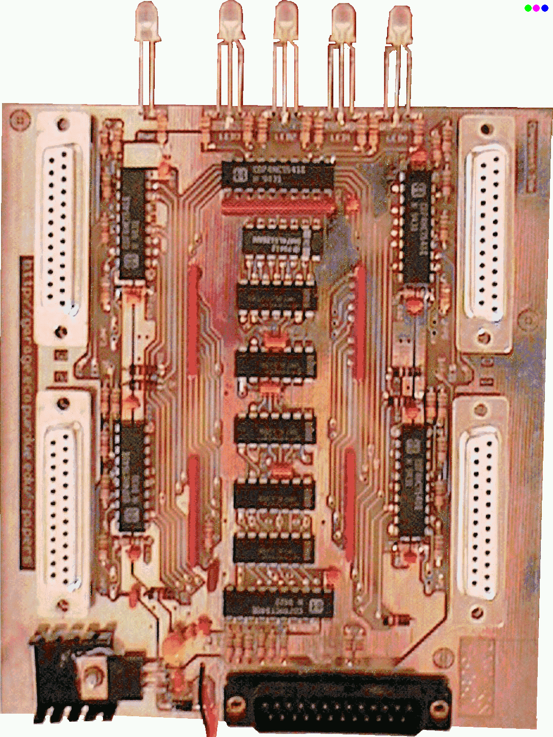
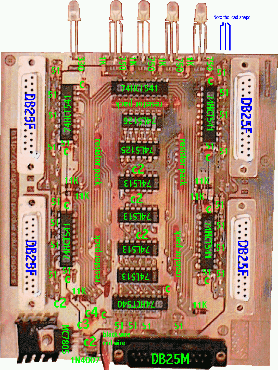
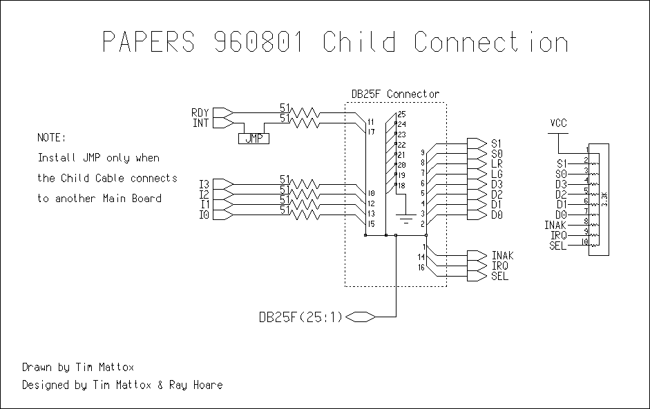
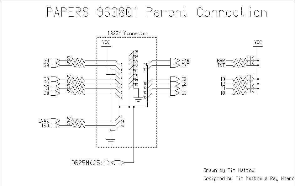
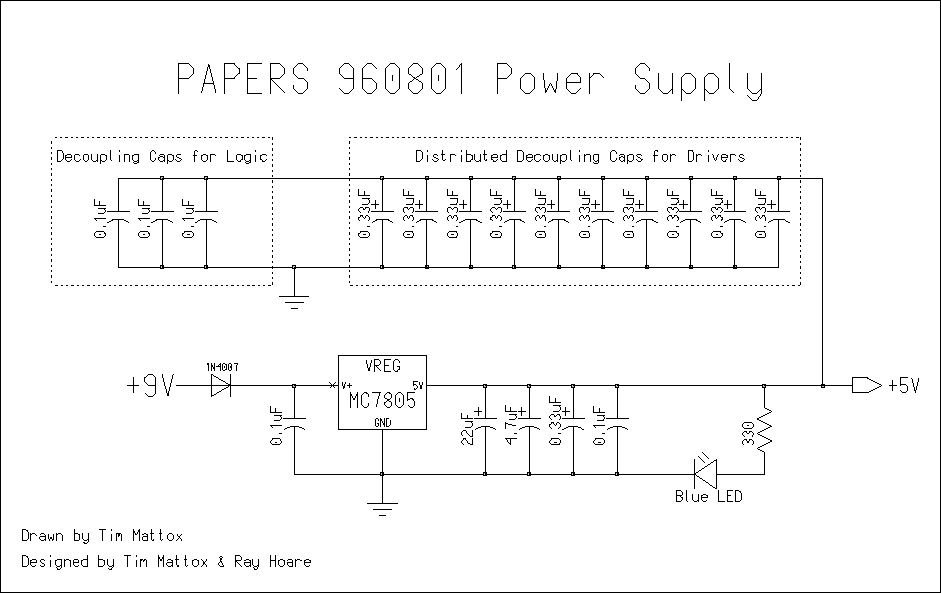
Here are two photographs of the 960801, without labels and with labels.
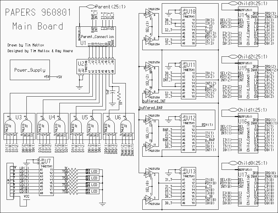
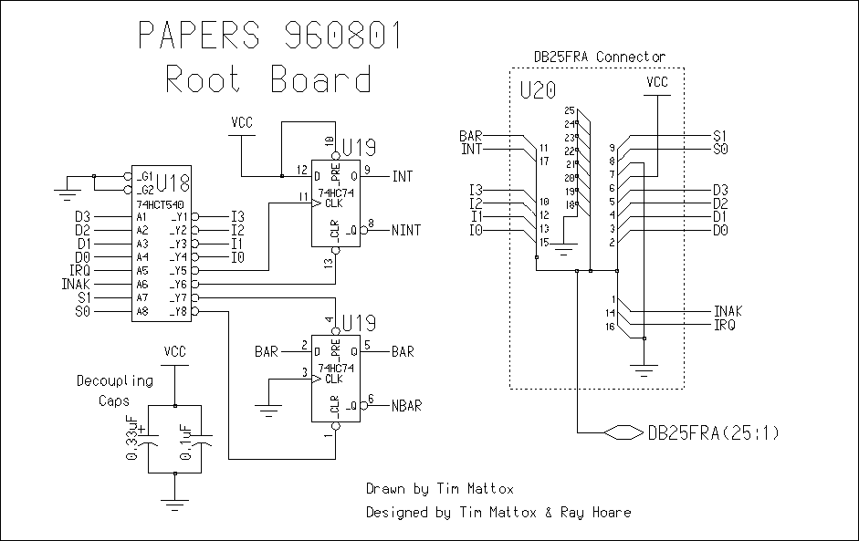
Schematics: main board, root board, child connection, parent connection, power supply.
4.1 Barrier Hardware
The barrier hardware logic is split between the Main Board and the
Root Board. The barrier signals S0, S1 originate from the PC and are
sent through pins 8 and 9 of the parallel port cable. They enter the
NAND gate of chip, U3 and then through the driver chip U2 through the
DB25M connector U1. For a four processor configuration, these signals
then enter the Root Node through pins 8 and 9 of the DB25F right angle
connector. They then travel through the inverting driver, U18, and
then S0 is sent to the _CLR input of the D flip flop, and S1 is sent
to the _PRE of the same D flip flop (chip U19). The output is then
sent out of the Root Node as BAR through pin 11 of the connector (U20)
into the connector U1 of the Main Board as BAR_T. From there is goes
into pins 3 and 6 of Chip U12. From pin 17 of U12, the signal is then
called "buffered BAR" and that signal enters pins 2, 5, 9, and 12 of
U8 which is a tri-state buffer. If the select line, SEL, is low then
the signal will enter the corresponding driver (U10, U11, U12 or U13,
depending on the which SEL line is set low) and will be sent back to
the PE through the RDY signal.
4.2 Interrupt Hardware
The interrupt logic is remarkably similar to the barrier logic, also
using a two 4-input NAND gates and a D flip-flop register. There is,
however, a difference in the connection between these chips.
Interrupt requests are generated by any PE, and acknowledged by all
PEs, while barrier synchronizations are always implemented by all PEs.
Thus, the input to the interrupt logic must be a logical OR of the IRQ
signals. Thus, to use a NAND gate to implement this function the
inputs, IRQ, must be active low. The interrupt must be acknowledge by
all PEs (using INAK) before processing is allowed to continue. Thus a
logical AND of the INAK signals must be performed. Fortunately the
input that sets the D flip-flop to low (the ~PRE input) is active low
and this allows the use of the NAND gate without modifying the
signals.
Finally, because there are not enough input bits for each PE, the
result from the barrier hardware and the result of the interrupt
hardware cannot be receive by the PE at the same time. The obvious way
to select between these values is using a multiplexer; however, there
is no standard 74-series part that implements selection between two
individual bits. Instead, the multiplexer is constructed using two
quad driver chips that have individually tri-stateable outputs. The
125 and 126 differ only in the sense of their enable lines, thus,
using the same select line to control one output on each chip makes it
possible to simply wire both outputs together. Only the selected
signal will be passed; the other line's driver will be in the
tri-state high impedance state. Thus, when the SEL line is set high
the interrupt register is readable on the RDY line and when SEL is
reset low the barrier register is readable on the RDY line.
The signals are IRQ, INAK, INT, RDY and SEL. IRQ requests an
interrupt, INAK acknowledges an interrupt and SEL selects the source
of the RDY signal which is equivalent to INT when SEL is high. An
interrupt is initiated by setting IRQ low, which is then propagated to
the U6 NAND chip. There is an RC circuit off of the output of the IRQ
NAND gate. This delays the signal so that spurious interrupts that are
due to noise are eliminated. The INAK signal is sent from the PE
through an inverting driver on the parallel port (built into the
Standard Parallel Port specification) and is an input to the INAK NAND
gate part of U6. The IRQ and INAK signals are then propagated through
inverting driver, U2, and set up the tree to the root node. On the
Root Board, the signal are received through the inverting driver and
sent to the interrupt flip-flop. The IRQ signal then clocks a "1" into
the flip-flop, U19, and onto the INT line. The INAK line is then used
to reset the same interrupt flip flop to low. The INT line is then
propagated down the tree to the Main Board. The signal enters the
driver U11, and is then placed into the inputs of tri-state buffers of
U9. Each of the SEL lines that come from each of the PEs and when set
high allows the INT signal to be propagated back to the PE through the
drivers (U10, U11, U12, or U13) to the RDY signal.
4.3 Aggregate Communication Hardware
Although AFAPI provides fancy communication primitives, they are all
built on top of four NAND trees and the barrier hardware. In the next
section some of the basic software libraries will be described but for
now the implementation of these NAND trees will be described.
For building a board that scales to only four processors, the NAND
trees are simply a 74LS13 chip. In general, there is nothing tricky
about building these NAND trees to scale to an arbitrary number of
processors except that the lines must be driven properly.
The aggregate communication hardware is very simple and is limited to
NAND chips U4 and U5. The inputs, D0..D3, come from each of the PEs,
are NANDed together and sent up the tree. Once they reach the root
node, they are unmodified and returned as I0..I3. On the Main Board
they are the I0_T..I3_T signals that enter the driver chips (U10, U11,
U12, or U13) and are sent back to the PEs.
4.4 LED Display Hardware
In the PAPERS prototypes, we have experimented with a variety of
different status displays. However, by far the easiest display to
understand was one using just a single bi-color LED for each
processor. The color code is very intuitive: green means running, red
means waiting (for more than two clock cycles), and black means not in
use. The problem is that there is no trivial way to derive these color
choices directly from the barrier logic, thus, the LEDs are explicitly
set under software control.
There are a variety of different types of bi-color LEDs, however, the
most common have three-leads: power for each of the two colors and a
common ground. The result is that each color of each LED must be
fairly well driven, and it isn't a good idea to make the computer port
directly drive the lights. Instead, a 74HC541 is used. For scaling,
each 74HC541 can handle all the LED drive for 4 processors.
There is also a blue power LED that indicates when power is plugged
in. However, we have found out that the blue power LED can actually
be turned on when the cables are plugged in and the power is NOT
connected. It turns out that under some very strange circumstances the
signal lines can be used to power the entire circuit even when the
power is not plugged in! Thus, in retrospect, the blue power LED
should be connected to the power between the 7805 and the power
diode. Therefore, the power should be plugged in first, the power LED
inspected, and then the signal cables should be plugged in.
It is also worth mentioning that, if you can't find appropriate
bi-color LEDs, you can simply use red LEDs and ignore the green LED
drivers. Likewise, if you can't find an appropriate blue LED for the
power indicator, a green LED can be substituted.
The LED signals, LR and LG, originate from the PEs and are sent to the
LED driver chip U7 and then through resistors to the LEDs. LR sets the
LED to red, LG set the LED to green and when both the LR and the LG
signals are high, the LED is orange.
4.5 Scaling
In the previous sections a four processor configuration has been
described. In this section, scaling to more than four processors will
be described. Scaling is very simple for this design and only
requires setting a single jumper and changing some of the cabling. For
any configuration, three more processors can be added to the system by
unplugging one of the PEs from a main board and inserting another Main
Board into that spot. There is a jumper that needs to be set but that
is all. The PE that was unplugged is then connected to the Main Board
that was just added.
More specifically, here is the procedure for adding another Main Board
to the system. A system of four or more processors is assumed to be
built and for sake of explanation, label the Main Board that is
already in the system the Internal Node and label the new Main Board
that we want to add, the Leaf Node. We will also label a specific PE,
the Leaf PE. For sake of simplicity, lets assume that the Leaf PE is
attached to U14 (even though it could be attached to U15, U16 or U17).
Now that we have defined our labeling scheme, here is the procedure
for adding the Leaf Node. Make sure that power is off for all of the
processors and for all of the PAPERS units. Disconnect the Leaf PE
from U14 and insert a M-F 25 conductor cable (straight through wiring
using DB25 connectors). Place a jumper on JMP3 that is next to U14
(this changes the signals that are sent to the U14). Now connect the
other end of the new cable to U1 of the Leaf Board and connect the
Leaf PE to U14 of the Leaf Board. There are now three extra
connections for PEs on the system, U15, U16, and U17 of the Leaf
Board. This procedure can be done as many times as needed and thus,
this design scales to over a thousand processors. It should be noted
that there is a performance cost of about 100ns with each tree level
that is added. This cost, however, is negligible compared to the 1us
that it takes for the processor to touch its parallel port.
As far as the signals are concerned, PAPERS 960801 is designed around
NAND gates and a few flip-flops. For an N processor system, this model
can be view in the abstract sense as using eight N-input NAND gates,
two flip-flops, N tri-state buffers and (6*N)+1 octal drivers. All of
the signals are ANDed as they travel up the tree and then are inverted
and sent back down the tree. At the root node the flip-flops control
the state of the barrier and interrupt logic but are also controlled
by an ANDing of the signals from the Main Boards.
4.6 Parts List
The complete parts list for constructing a PAPERS 960801 is given in
Table 5. The total parts cost for a unit should be between $50 and
$100, depending on the quantity and source for the parts. For example,
the cables can be purchased for less than $2 each via mail order, but
can be more than $20 each if purchased from some stores. We strongly
recommend checking prices from several mail order sources for cables
and other parts.
Along the same lines, if your computers do not have unused parallel
printer ports, there is a very wide range in the pricing of ISA bus
parallel port cards. We have found a $7 card via mail order that works
fine; the $45 or more that you would spend for each card in some
stores isn't likely to buy you any improvement in performance. In
fact, if there is a speed difference between the card and the built-in
port, it is harmless to use the slower port for a printer while the
faster port is used for the PAPERS 960801 connection. Do not use a
port-switcher or similar device to share a single port; PAPERS 960801
might not work with such devices.
| Qty |
Description |
Label |
Used In |
Part Number |
Source |
| 32 |
51 Ohm resistors |
51 |
Connection |
R51 |
JDR |
| 1 |
330 Ohm resistor |
LB |
Display |
R330 |
JDR |
| 4 |
750 Ohm resistor |
LG |
Display |
R750 |
JDR |
| 5 |
1K Ohm resistor |
LR, 1K |
Display, Logic |
R1.0K |
JDR |
| 5 |
10 pin SIP, 3.3k resistor, bussed |
+ |
Connection |
RPS9-3.3K |
JDR |
| 6 |
11K Ohm resistors |
11K |
Connection |
R11K |
JDR |
| 1 |
0.001 uf Capacitor (non-electrolytic) |
cap |
Logic |
.001UF-MONO |
JDR |
| 1* |
0.1 uf capacitor (non-electrolytic) |
|
Power |
.1 UF-MONO |
JDR |
| 5 |
0.1 uf Capacitor (non-electrolytic) |
|
Power |
.1 UF-MONO |
JDR |
| 1* |
0.33 uf Tantalum cap. |
|
Power |
T.33-35 |
JDR |
| 11 |
0.33 uf Tantalum Cap. |
|
Power |
T.33-35 |
JDR |
| 1 |
4.7 uf Tantalum Cap. |
|
Power |
T4.7-16 |
JDR |
| 1 |
22 uf Tantalum Cap. |
|
Power |
T22-10 |
JDR |
| 1 |
1N4007 Power Diode |
|
Power |
1N4007 |
JDR |
| 1 |
7805, 5 volt regulator |
|
Power |
7805T |
JDR |
| 4 |
3-lead Bi-Color Red/Green LED |
LED0-LED3 |
Display |
LT1057-ND |
DigiKey |
| 1 |
Blue LED |
Blue |
Display |
LED103 |
JDR |
Table 5a: PAPERS 960801 Module Parts List � Discrete
Components
| Qty |
Description |
Label |
Used In |
Part Number |
Source |
| 1* |
74LS74 dual D Flip-flop |
U19 |
Logic |
74LS74 |
JDR |
| 4 |
74LS13, dual 4-input NAND |
U3-U6 |
Logic |
74LS13 |
JDR |
| 1 |
74LS125, quad Tri-State Buffer |
U8 |
Logic |
74LS125 |
JDR |
| 1 |
74LS126, quad Tri-State Buffer |
U9 |
Logic |
74LS126 |
JDR |
| 5 |
74HCT541, octal Driver |
U7, U10-U13 |
Display, Connection |
74HCT541 |
JDR |
| 1* |
74HCT540 inverting octal Driver |
U18 |
Logic |
74HCT540 |
JDR |
| 1 |
74HCT540, inverting octal Driver |
U2 |
Connection |
74HCT540 |
JDR |
Table 5b: PAPERS 960801 Module Parts List - ICs
| Qty |
Description |
Label |
Used In |
Part Number |
Source |
| 4 |
6-10', 25-wire M-M DB25 |
|
Cables |
|
|
| 1 |
Circuit Board (Fig. xxx) |
960801 |
Logic |
|
|
| 1 |
Root Circuit Board |
Root |
Logic |
|
|
| 4 |
DB25 Female Connectors |
U14-U17 |
Connection |
DB25SC |
JDR |
| 1* |
DB25 RA Female Connector |
U20 |
Connection |
DB25SRS |
JDR |
| 1 |
DB25 Male Connectors |
U1 |
Connection |
DB25PC |
JDR |
| 4 |
Jumper, 0.1" spaced |
JMP0-JMP3 |
Connection |
JUMPER |
JDR |
| 1 |
9-12 volt, 500mA AC-DC adapter |
|
Power |
TR09-DC2.5 |
JDR |
| 1 |
Power receptacle |
|
Power |
PC25S |
JDR |
| 1 |
22 AWG Red Power Wire, ~1' |
|
Power |
|
|
| 1 |
22 AWG Black Power Wire, ~1' |
|
Power |
|
|
| 1 |
7805 Heat Sink, .75" by .75" |
|
Power |
HS507302B |
JDR |
| 1 |
Heat Sink Compound |
|
Power |
|
|
| 1 |
#256 Screw, lock washer, nut |
|
Power |
|
|
Table 5c: PAPERS 960801 Module Parts List � Misc.
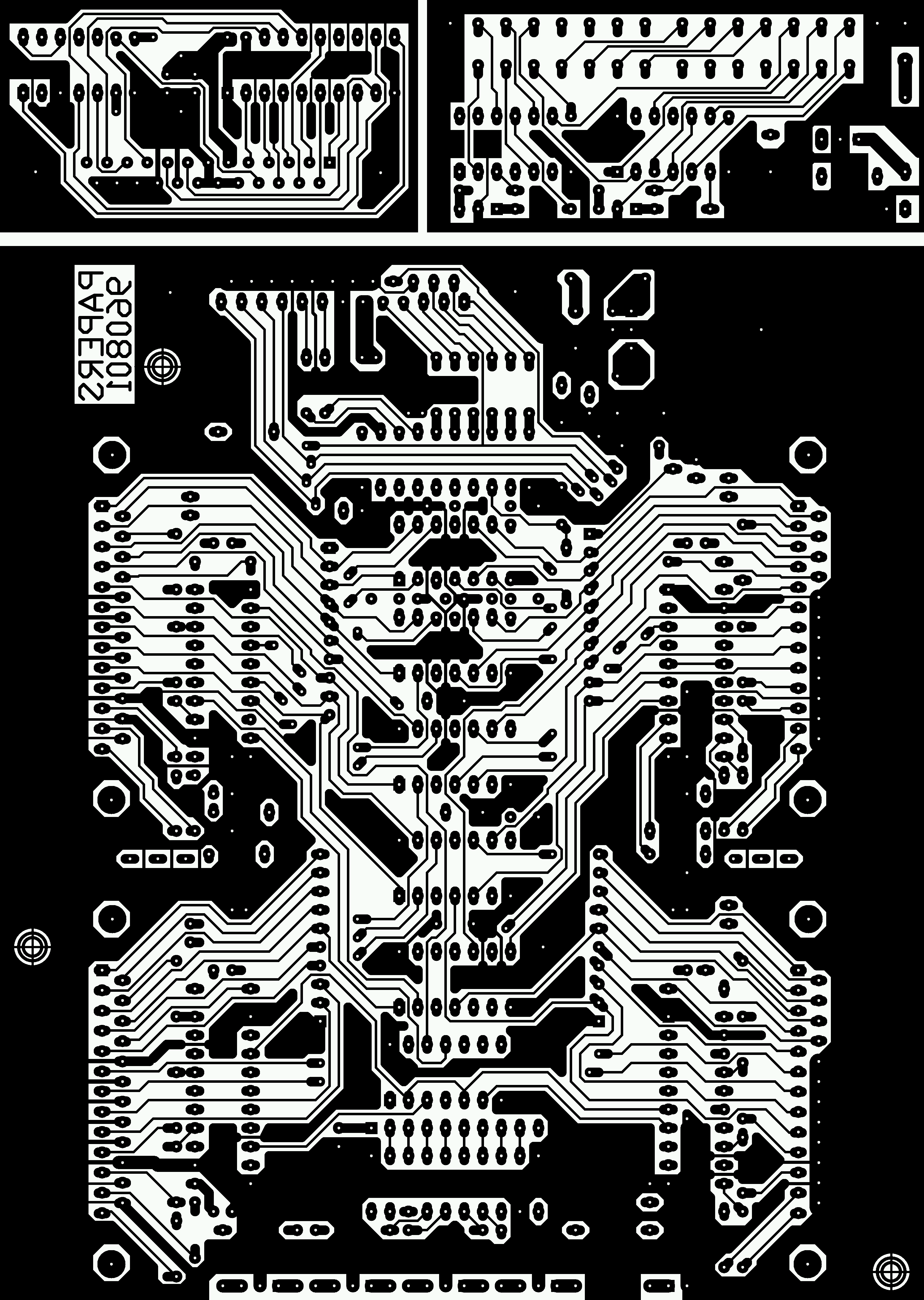
4.7 Using Our Board Masks
Although you can make your own board masks, if you would like
to fab your own boards using our masks, you are welcome to do
so. Here's a brief overview of how.
Because the 960801 main module boards in general require root
boardlets as well, the board masks actually include both
the main module board and the root boardlet in a single mask
set; in fact, there is even a bit of extra space left in
making that combined mask rectangular, so there is even a
wimpy two-processor-only PAPERS version in the remaining
corner of the mask, all with the fab perforated so that the
boards are easily detached. Feel free to discard the
two-processor board; it was either that or use the space to
make keychains... which in retrospect might have been more
useful....
The board masks were created using EasyTrax, and our full
design files are freely available online in this directory. As explained by the README file in that directory,
these files include the Gerber
top layer, Gerber bottom
layer, and Gerber
apeture files.
Although we do not recommend it, you could actually produce the
boards yourself using just a good-quality printer, PC-board
making kit, drill press, and a lot of hand labor. If you wish
to go this route, here are suitable postscript and 600DPI GIF
images of the top layer (.ps, .gif) and the bottom layer (.ps, .gif). For reference, a 100DPI
GIF of the top layer is:

A 100DPI GIF of the bottom layer is:

You would use the postscript or 600DPI images to print
high-quality hardcopy suitable for making your PC-board kit
masks. Using a typical kit, after the boards have been
etched, you hand drill the holes -- a task which is time
consuming, but relatively painless. The really bad news is
that this board has over 700 plated-through holes,
which you would have to implement by one of several rather
painful techniques, such as hand-soldering short wires through
each of these holes. Note: only do this for holes that are not
for a component's pin. For component pin holes, you will
have to solder to both sides of the board if there is a trace
on the compnent side.
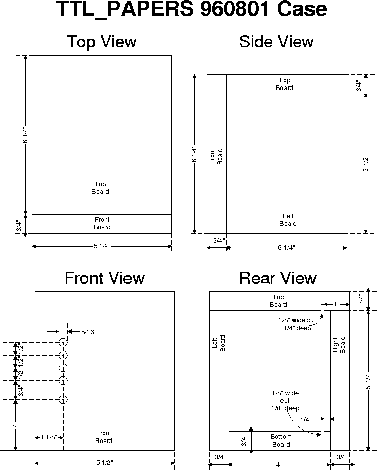
4.8 The Board Frame
Ok, so you have made boards according to our specifications
(i.e., as per the masks). Now there is the little issue of
building a box to hold them. Actually, the easiest and most
functional box is nothing more than an open frame made from 3
pieces of standard-sized 1-by lumber. When finished, it looks
like:
Two of the blocks can be cut from 1x4 (really 3/4" x 3 1/2")
stock, one piece 1 1/2" long and the other 7" long. The third
block is cut from 1x6 (really 3/4" x 5 1/2") stock to a length
of 6". The 1st and 3rd blocks are then slotted as shown below
(e.g., using a table saw). Finally, the three parts are
screwed and/or glued together as:

To make this even clearer, we have posted full-size postscript
files for the Top View, Front View, and Right SIde View. This open frame
shows-off the PAPERS hardware, while providing full access to
the connectors on the board. The base is just wide enough to
ensure that the weight of the cables will not tip the frame.
If the rather modern appearance of the open frame bothers you,
here is an alternative design,
yielding a much more conventional-looking box.
5. PAPERS Software
See http://aggregate.org/AFAPI/
6. Conclusion
In this paper, we have presented the complete public domain design of
the PAPERS 960801 hardware. This design represents the simplest
possible scalable mechanism to efficiently support barrier
synchronization, aggregate communication, and group interrupt
capabilities using unmodified conventional workstations or personal
computers as the processing elements of a fine-grain parallel machine.
We do not view PAPERS 960801 as the ultimate mechanism, but rather as
an introductory step toward the more general and higher performance
barrier and aggregate communication engines that have been at the core
of our research since 1987. The key thing to remember about PAPERS
960801 is not what it is, but rather why it is.
- Why is PAPERS 960801 so much lower latency than other networks?
-
Because it doesn't have a layered hardware and software interface.
- Why is the hardware so simple?
-
Because it isn't a network; the fact that PAPERS 960801 communications
are a side-effect of barrier synchronization eliminates the need for
buffering, routing, arbitration, etc.
- Why is it useful?
-
Because, although shared memory and message passing hardware is very
common, the most popular high-level language and compiler models for
parallelism are all based on aggregate operations exactly what PAPERS
960801 provides. Further, barrier synchronization is the key to
efficiently implementing MIMD, SIMD, and VLIW mixed-mode execution.
- Why didn't somebody do it earlier?
-
We and others did. The problem is that tightly coupled design of
hardware and compiler is not the standard way to build systems, so
earlier designs (e.g., PASM, TMC CM-5) tended to use too much hardware
and interface software, cost too much, and perform too poorly.
- Why is it public domain?
-
Two reasons: (1) Purdue University didn't want to patent the basic
mechanism back in 1987 and (2) we are primarily interested in the
related compiler technology, and having more appropriate hardware
makes our compiler work more valuable (i.e., more publishable).
Higher-performance versions of PAPERS are on the way. In fact, this
PAPERS 960801 design is the eleventh PAPERS design we have built and
tested, and three of the other designs easily outperform it... but
they use much more hardware. We are currently working on a smart
parallel port card for the ISA bus that will roughly quadruple the
performance of PAPERS 960801 without any change to its hardware. We
are also pursuing versions of the higher-performance designs based on
Texas Instruments FPGAs, and anticipate a PCI interface to future
PAPERS units. Also watch for releases of various compilers targeting
PAPERS. The email server at papers@ecn.purdue.edu will be the primary
place for announcing and distributing future releases of both hardware
and software.
References
Schematics: main board, root board, child connection, parent connection, power supply.
[CoD94] W. E. Cohen, H. G. Dietz, and J. B. Sponaugle, Dynamic Barrier Architecture For Multi-Mode Fine-Grain Parallelism Using Conventional Processors; Part I: Barrier Architecture, Purdue University School of Electrical Engineering, Technical Report TR-EE 94-9, March 1994.
[CoD94a] W. E. Cohen, H. G. Dietz, and J. B. Sponaugle, Dynamic Barrier Architecture For Multi-Mode Fine-Grain Parallelism Using Conventional Processors; Part II: Mode Emulation, Purdue University School of Electrical Engineering, Technical Report TR-EE 94-10, March 1994.
[CoD94b] W. E. Cohen, H. G. Dietz, and J. B. Sponaugle, "Dynamic Barrier Architecture For Multi-Mode Fine-Grain Parallelism Using Conventional Processors," Proc. of 1994 Int'l Conf. on Parallel Processing, St. Charles, IL, pp. I 93-96, August 1994.
[DiC94] H. G. Dietz, W. E. Cohen, T. Muhammad, and T. I. Mattox, "Compiler Techniques For Fine-Grain Execution On Workstation Clusters Using PAPERS," 7th Annual Workshop on Languages and Compilers for Parallel Computing (also to appear as a book chapter from Springer Verlag), Cornell University, August 1994.
[DiM94] H. G. Dietz, T. Muhammad, J. B. Sponaugle, and T. Mattox, PAPERS: Purdue's Adapter for Parallel Execution and Rapid Synchronization, Purdue University School of Electrical Engineering, Technical Report TR-EE 94-11, March 1994.
[DiO92] H. G. Dietz, M.T. O'Keefe, and A. Zaafrani, "Static Scheduling for Barrier MIMD Architectures," The Journal of Supercomputing, vol. 5, pp. 263-289, 1992.
[DiH96] "A Fine-Grian Parallel Architecture Based on Barrier Synchronization," Proc. of 1996 Int'l Conf. on Parallel Processing, St. Charles, IL, pp. I247-250, August 1996.
[Jor78] H. F. Jordon, "A Special Purpose Architecture for Finite Element Analysis," Proc. Int'l Conf. on Parallel Processing, pp. 263-266, 1978.
[OKD90] M. T. O'Keefe and H. G. Dietz, "Hardware barrier synchronization: static barrier MIMD (SBM)," Proc. of 1990 Int'l Conf. on Parallel Processing, St. Charles, IL, pp. I 35-42, August 1990.
[OKD90a] M. T. O'Keefe and H. G. Dietz, "Hardware barrier synchronization: static barrier MIMD (DBM)," Proc. of 1990 Int'l Conf. on Parallel Processing, St. Charles, IL, pp. I 43-46, August 1990.
[SiN87] T. Schwederski, W. G. Nation, H. J. Siegel, and D. G. Meyer, "The Implementation of the PASM Prototype Control Hierarchy," Proc. of Second Int'l Conf. on Supercomputing, pp. I 418-427, 1987.
 The only thing set in stone is our name.