
In class, referencing Appendix B of the text, we began by describing how registers and main memory are constructed in terms of the EE280-level logic involved. We also discussed how tri-state logic is used to interface to busses and how a decoder can be used to select a particular register within a register file. After discussing these things, we moved into the design of a simple processor.
The text does not discuss this simple processor design, so the discussion from class is summarized here as a reference that you can use to answer homework problems, etc. The design here is a single-bus processor architecture, as described in class, which can implement essentially the same MIPS subset ISA that we will use throughout the course. (Pages 152 and 228 of the text describe this subset, but we will ingore the byte load and store.)
Recall that the processor interfaces to memory as:

The read/~write line is a 1 for reading, 0 for writing. Strobe is pulsed when the memory address lines are valid. If the operation is a read, then MFC is set by the memory when it has completed fetching (reading) data for the processor, at which time data becomes valid for the processor to use.
Before discussing the processor architecture, it is useful to note that there is now a complete cycle-by-cycle simulator available via a WWW form interface at https://aggregate.org/cgi-bin/simple.cgi. That simulator can be used to write and test your own control sequences.
Inside the processor, there are a variety of function units and registers connected to each other by one or more datapaths (e.g., busses). The control is responsible for sequencing the RTL (register transfer level) operations that implement each instruction in the ISA (instruction set architecture). Let's look inside this very simple implementation of the processor:
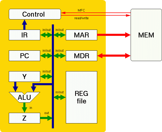
The red lines communicate between the processor and the memory. Blue lines are internal, dedicated, electrical connections; in contrast, green lines represent connections that can be made or broken as the control specifies. Let's look at each of the control signals and define what they mean:
| REGISTER control signal | Effect |
|---|---|
| ALUadd | Configures the ALU to add its inputs |
| ALUand | Configures the ALU to bitwise AND its inputs |
| ALUxor | Configures the ALU to bitwise eXclusive OR its inputs |
| ALUor | Configures the ALU to bitwise OR its inputs |
| ALUsll | Configures the ALU to shift left logical; the result is (bus << Y) |
| ALUslt | Configures the ALU to compare its inputs; the result is (Y < bus) |
| ALUsrl | Configures the ALU to shift right logical; the result is (bus >> Y) |
| ALUsub | Configures the ALU to subtract the buss input from Y |
| CONST(value) | Places the constant value onto the bus |
| HALT | Halt the machine (stop the simulator without error) at the end of the current state |
| IRaddrout | Tri-state enables the portion of the Instruction Register that contains the (26 bit, MIPS "J" format) address, along with the top 6 bits of the Program Counter, to be driven onto the bus |
| IRimmedout | Tri-state enables the portion of the Instruction Register that contains the (16 bit, MIPS "I" format) 2's complement immediate value to be sign-extended to 32 bits and driven onto the bus |
| IRin | Latches the bus data into the Instruction Register at the trailing edge of the clock cycle |
| IRoffsetout | Tri-state enables the Instruction Register's shifted and sign extended value from the offset field to be driven onto the bus (used for branches) |
| JUMP(label) | Microcode jump to label |
| JUMPonop | Microcode jump to label named like the opcode; e.g., if an "Addi" is in the IR, jumps to the microcode label Addi |
| MARin | Latches the bus data into the Memory Address Register at the trailing edge of the clock cycle |
| MARout | Tri-state enables the Memory Address Register's output to be driven onto the bus |
| MDRin | Latches the bus data into the Memory Data Register at the trailing edge of the clock cycle |
| MDRout | Tri-state enables the Memory Data Register's output to be driven onto the bus |
| MEMread | Initiate a memory read from the address in the MAR; here, you may assume that the memory will take 2 clock cycles to respond |
| MEMwrite | Initiate a memory write using the data in the MDR and the address in the MAR; in this simple design, you may assume that a memory write takes precisely 1 clock cycle |
| PCin | Latches the bus data into the Program Counter at the trailing edge of the clock cycle |
| PCinif0 | Only if the value in Z is zero, latch the bus data into the Program Counter at the trailing edge of the clock cycle |
| PCout | Tri-state enables the Program Counter's output to be driven onto the bus |
| REGin | Latches the bus data into whichever register is selected by SELrs, SELrt, or SELrd; the value is latched at the trailing edge of the clock cycle |
| REGout | Tri-state enables the output of whichever register is selected by SELrs, SELrt, or SELrd; the selected value is driven onto the bus |
| SELrs | Selects the rs field of the IR to be used to control the register file's decoder |
| SELrt | Selects the rt field of the IR to be used to control the register file's decoder |
| SELrd | Selects the rd field of the IR to be used to control the register file's decoder |
| UNTILmfc | Repeat this state until the memory has issued a memory fetch complete signal, indicating that the fetched value will be valid to read from the MDR in the next clock cycle |
| Yin | Latches the bus data into the Y register at the trailing edge of the clock cycle; this register is needed because, with only one bus, one of the two operands for a binary operation (e.g., Add) must come from somewhere other than the bus |
| Yout | Tri-state enables the Y register's output to be driven onto the bus |
| Zin | The ALU is always producing a result, but we only make note of that result if we latch the ALU's output into the Z register at the trailing edge of the clock cycle |
| Zout | Tri-state enables the Z Register's output to be driven onto the bus |
Consider the MIPS instruction add $8,$2,$5, which, when executed, should make register $8 = ($2 + $5). The 32-bit pattern encoding this instruction is:
| op | rs | rt | rd | shamt | funct |
|---|---|---|---|---|---|
| 0 | 2 | 5 | 8 | 0 | 32 |
The simulator would allow you to specify this Add instruction's bit pattern as (rs(2)+rt(5)+rd(8)+funct(32)), which is just a pretty way to say 0x00454020. (Note that 0x is used to prefix a hexadecimal value, just as in the C language.)
What Register Transfer Level (RTL) operations would we need to perform in order to get this work done?
First, let's think about the "guts" of the operation: the add. In order to add, we have to get the appropriate values at the ALU inputs, tell the ALU to add, latch the result, and copy the latched result into the destination register. That work can be done by:
That's all well and good, but how did the processor know it was supposed to add? In order to know that, it must first fetch the instruction from main memory (or a cache) and decode it:
Let's consider that last operation more closely. How does JUMPonop know how to decode the instruction? Well, for our simulator, the answer is quite simple: you tell it. Basically, you label each location that you might want JUMPonop to jump to and you specify when each label is to be that target. The when specification for the simulator are very straightforward, specifying mask and match values. If ((IR & mask) == match), then label is the next state. So, we could specify the add decode as:
when (op(0x3f)+funct(0x3f)) funct(32) Add
Basically, this says that when the op and funct fields of the IR are, correspondingly, 0 and 32, we are looking at a MIPS add instruction and JUMPonop should go to the label Add.
Obviously, the above control sequence takes a minimum of 4 clock cycles to execute (1 tick per set of RTL operations). However, the UNTILmfc operation may cause state 2 above to be repeated many times if the memory read is relatively slow, so 4 is just the minimum number of ticks. The JUMPonop would then bring us to the set of RTL operations that implements the instruction (in our case, the RTL labeled "Add"). These first 4 states really have nothing to do with the opcode being Add -- they simply fetch the instruction and bump the PC to point at the next instruction. All instructions can share these first 4 states.
Thus, we now know how the processor will get to our add code. However, once the add is done, how will the processor get to the next instruction? One answer is to do this:
Start:  PCout, MARin, MEMread
        UNTILmfc
        MDRout, IRin
        JUMPonop

	/* other stuff goes here... */

Add:    SELrs, REGout, Yin
        SELrt, REGout, ALUadd, Zin
        Zout, SELrd, REGin
        /* increment PC by 4 and start next instruction */
        PCout, Yin
        CONST(4), ALUadd, Zin
        Zout, PCin, JUMP(Start)
Ok, that's a working solution. However, it would result in just about every instruction type ending with copies of those same last 3 states. Aside from saving some microprogram space, factoring out this sequence should allow us to take advantage of the fact that the PC value was already on the bus in the state labeled Start. It is important to note that incrementing the PC early is harmless because MIPS operations that store other values into the PC (e.g., jumps and branches) will simply overwrite the incremented value. Consider this clever interleaving of the next instruction sequence with the start of instruction RTL:
Start:  PCout, MARin, MEMread, Yin
        CONST(4), ALUadd, Zin, UNTILmfc
        MDRout, IRin
        Zout, PCin, JUMPonop

	/* other stuff goes here... */

Add:    SELrs, REGout, Yin
        SELrt, REGout, ALUadd, Zin
        Zout, SELrd, REGin, JUMP(Start)
We've just saved 3 clock ticks. One might be concerned that the UNTILmfc operation causes "CONST(4), ALUadd, Zin" to be repeated, perhaps many times. However, this is harmless: the exact same result is computed in each repeat of the RTL set, with no harmfull side effects. For example, it might not be acceptable to repeat a state that contains MEMread because issue of multiple MEMread stobe signals could confuse the memory system.
There are two lessons to be learned here:
Ok. So now we know how to execute an Add. How many clock cycles will it take to execute one instruction -- i.e., what is the CPI?
Clearly, each state (line of RTL) that is entered will take at least one clock cycle: 10 for our first version and 7 for the improved version. However, the UNTILmfc operation is essentially a repeat-until loop that repeats the processor control state it is in until memory has responded to a MEMread request. In our examples above, the UNTILmfc occurs in the state immediately after the MEMread is issued. Thus, if memory takes M clock cycles to respond, the line containing UNTILmfc will be repeated M times, not just executed once. If M is 5, our examples respectively would yield 15 CPI and 12 CPI.
As we just demonstrated, merely rearranging RTL operations can significantly change the CPI. Basically, getting more work done per clock cycle is the trick, and that's largely a matter of using parallelism. What paralleism? Well, in the above example we achieved some speedup by repacking RTL operations to have the processor literally do more useful work in each state, but we also can improve paralleism by increasing the overlap period in which both the processor and memory are working:
Start:  PCout, MARin, MEMread, Yin
        CONST(4), ALUadd, Zin
        Zout, PCin, UNTILmfc
        MDRout, IRin, JUMPonop
        ...

Add:    SELrs, REGout, Yin
        SELrt, REGout, ALUadd, Zin
        Zout, SELrd, REGin, JUMP(Start)
By rearranging things a bit more, we did not reduce the total number of states used in describing the Add instruction, but we did increase overlap with memory operation. In this version, the UNTILmfc is separated from the MEMread by an additional state. Thus, the first clock cycle of memory delay overlaps the execution of CONST(4), ALUadd, Zin, thus saving one clock cycle of UNTILmfc repetition. The result would be 11 CPI.
Of course, when we talk about performance of a processor, we have to consider CPI for all types of instructions, not just Add. Many modern processors do so much work in each clock cycle that the CPI are often fractions less than 1; in such cases, we talk about IPC: Instructions Per Cycle.
How fast can the processor clock be? The answer is determined by the propogation delays in the processor's circuits. Consider the state:
SELrt, REGout, ALUadd, Zin
Let's use times approximating what you would get physically building the above circuits using logic parts like those employed in a course like EE481. SELrt is running through a decoder, which might take 10ns. When the REGout control signal is set at the start of this clock cycle, it might take about 5ns for a value to propogate to the bus. Thus, some value is on the bus after 5ns, but it might take 10ns+5ns=15ns before the correct value is on the bus. Similarly, the ALU is adding incorrect values until 15ns; so a 30ns ALU would yield correct results at the 15ns+30ns=45ns mark. Zin happens at the end of the clock period, but might require its input to have been stable for 5ns in order to latch it. Thus, we get 45ns+5ns=50ns as the fastest allowable clock period, for a maximum clock frequency of 20MHz.
In the above example, all the operations were on the same path; it is generally possible that there are multiple separate or branched circuit paths within a single clock cycle:
SELrt, REGout, ALUadd, Zin, MARin
This example has two paths: one is the SELrt->REGout->ALUadd->Zin path just described, the other is the SELrt->REGout->MARin path. In such a case, the slowest path determines the maximum clock frequency. In fact, because the same clock frequency is used for all states, the slowest path in any state is that critical path that determines the maximum clock frequency. Keep in mind that the slowest path might not be the path affected by the most control signals: if MARin took more than 35ns (which is admittedly very unlikely), then SELrt->REGout->MARin would be slower than SELrt->REGout->ALUadd->Zin.
Obviously, using faster logic parts can shorten the critical path and thus permit a higher clock frequency. However, merely rearranging how RTL operations are allocated to states also might allow use of a higher clock frequency. Ideally, we want operations to be arranged so that all states have about the same slowest path time.
How might we rearrange things to increase the clock speed? Well, consider re-writing the above single state as two states:
SELrt, REGout, MARin
MARout, ALUadd, Zin
Using our EE481-based times, SELrt->REGout->MARin would take about 10ns+5ns+5ns=20ns and MARout->ALUadd->Zin would take about 5ns+30ns+5ns=40ns. Thus, if our original state was the clock limiting factor, we could now increase the clock frequency from 20MHz to 25MHz! Of course, the problem with that is that now we have 12CPI instead of 11CPI, so things didn't speed-up as much as one might have hoped.... This is a very common problem: Clock speed and CPI tend to trade-off against each other such that improving one hurts the other. A good real-world example is the AMD Athlon vs. the Intel Pentium 4: the Althon maximizes work done per clock at the expense of a slower clock, the Pentium 4 trades a faster clock for getting less work done per tick.
Suppose that we wanted to go even further in favor of accelerating the clock? The ALU is probably the slowest thing in any pipeline, so why not try to make it faster? As we'll discuss later in the course, you can get some speedup by throwing more circuitry at the problem. However, you also can break-up the operation of the ALU over multiple clock cycles. For example, instead of the above split of that original state into two, one could reduce the slowest path to a mere 10ns by something very much like:
SELrt
SELrt, REGout, ALUadd, MARin
SELrt, REGout, ALUadd
SELrt, REGout, ALUadd
SELrt, REGout, ALUadd, Zin
Here, SELrt completes in the first cycle. Thus, REGout can have a stable correct decoder value from the start of the second cycle, allowing REGout and MARin to complete -- along with the first 5ns of ALUadd delay. The third and fourth cycles just hold inputs steady for the adder to continue its work. Finally, halfway through the fifth cycle, the adder completes and Zin latches the result. Of course, dividing a 50ns path into 5 cycles with 10ns paths by itself doesn't improve the processor's performance at all, but you do get to brag about having a 100MHz clock.... If you're lucky, some other original states will turn into fewer than 5 states each, so you will get speedup on them.
Actually, the principle of subdividing long logic paths is not as scalable as it first appears. One purely analog problem is that a clock signal that must be distributed to many circuit components cannot be made arbitrarily fast. A more digital problem is that, as modules are subdivided, to avoid glitches, it may be necessary to latch the partial results at the end of each clock and re-issue them at the start of the next clock. The portion of a module between latches is called a stage. When we carve-up a 30ns module, we might get 5ns+5ns latch times added for each stage. Thus, our original 30ns module might yield two 25ns pieces, three 20ns pieces, six 15ns pieces, etc. In fact, this is precisely the kind of thing pipelining does -- but it also takes advantage of the fact that those latches allow the now isolated stages to work on different data at the same time: parallel execution of portions of six operations for a six-stage pipeline. That's what the more modern processor architecture later in the course is all about....
In case you had not guessed, the simulator allows you to test arbitrary control sequences like we've described above. However, it does not allow a single function unit's execution to span clock cycles (after all, we just told you that trick was prone to glitches, etc.).
A specification for the simulator consists of delay and when specifications, control states, and initial/final values for registers and memory locations. There should be an example pre-loaded in the form. Play with it. Enjoy. Let me know if there are problems.... Here's a bit more detail about the simulator's input.
The simulator input is line-oriented, with the end-of-line serving as a separator between commands. Alternatively, multiple commands can be specified on a single line using semicolon (;) as a separator. Comments can be parts of a line or even multi-line using the conventional C comment style (start with /* and end with */), or can be until the end of the line using either -- or //. Because some people like commas between signal names, commas are treated just like spaces.
Integer values can be specified using most of the usual C expression notation. Supported binary operators include: |, &, ^, <, <=, >, >=, ==, !=, <<, >>, +, -, *, /, and %. Supported unary operators include: !, -, ~, and field constructor functions op(expr), rs(expr), rt(expr), rd(expr), shamt(expr), funct(expr), addr(expr), and immed(expr). The field constructors shift and mask their arguments to fit them into the bitfields of the same names within the MIPS instruction format. Constants can be specified as hexadecimal (prefixed by 0x), decimal (the default), octal (0 followed by octal digits), or even binary (prefixed by 0b). For example, the value ten could be written as 0xa, 0xA, 10, 012, or 0b1010.
New for Spring 2005, the simulator now supports specification of signal delays and automatic computation of critical path delays and minimum allowable clock period. The delays are tracked as integer values, which one might typically interpret as either microseconds or nanoseconds. The specification syntax is straightforward: delay expr list_of_signals. All the signal names defined above can have integer delays specified. In addition, SEL can be used to specify the time to be used for all selects, OUT for all outputs, IN for all inputs, and ALU for all ALU operations. These delay specifiations are processed in order, thus, delay 5 SEL; delay 10 SELrd; is valid shorthand for delay 5 SELrs SELrt; delay 10 SELrd;. Signal delays not specified default to a value of 0.
The delay specification also allows the WWW interface-specified memory read latency in clock cycles to be overridden with a clock cycle count computed from the raw memory read delay and the computed critical path delay. The memory read delay is reprsented by MEM in a delay specification. For example, if the minimum allowable clock period is found to be 35, then delay 100 MEM; would cause all memory reads to take 3 clock cycles; a minimum allowable clock period of 10 would make the same specification result in a 10 clock cycle latency for a memory read.
As suggested above, when specifications are used to decode instructions when JUMPonop is triggered. A when x y z; means go to state z next when (IR&x)==y. Like delay specications, when specifications are processed in the order specified; the result is that ambiguous specifications always use earliest specified when that is satisfied. If no when is satisfied, JUMPonop becomes a null operation and the next state in sequence is the next state.
Really no surprises here; just list the signals you want in each state. A state may be prefixed by a symbolic labels followed by a colon, e.g., the start state begins with Start:. The parser does simple checks for illegal combinations of control signals within a state, so it can warn of such things even if no simulation is performed.
Testing that your state machine does what you want requires simulating execution of some instructions. For this purpose, the simulator allows you to specify arbitrary initial and final states for any of the registers and memory locations.
The registers are IR, PC, MAR, MDR, Y, Z, and $expr; the last notation is used to specify a register number, 0-31. Registers that don't have initial values specified are set to a default initial value of 0. Memory locations work differently -- memory locations literally do not exist until you initialize them or your program stores into them. Each memory location is four byte addresses long and must be aligned on a multiple of four boundary. Thus, the first memory word is MEM[0] and the second is MEM[4]. However, you need not access or define memory locations in sequence; any MEM[expr] can be initialized in any sequence.
Initializing a register or memory location is done using something closely resembling an assignment statement allowing an expression on the right side. For example, PC=7+1; sets the PC to initially have the value 8.
However, the simulator also allows specification of final values. These values are intended primarily for the TA to use in grading assignments... after all, it is difficult to consistently grade code without using functional tests. Thus, each final value specification looks a lot like an initialization with three differences: the # symbol is used instead of =, there are two expressions on the right hand side instead of just one, and memory locations are handled specially. The second expression is used to specify how many points to take off if the specified value does not match. For example, PC#12 10; would say that having the final value of the PC equal to 12 is worth 10 points. The final score is reported as a weighted percentage match for all stated final conditions followed by a list of which values were incorrect.
Final values for memory locations are specified using MEM[expr]#expr;, with only one argument on the right side. The cost weighting for a mismatch is specified for all memory locations using MEM#expr to set the cost for all memory mismatches. This is done because one of the most common types of memory mismatch is changing the value of a memory location that shouldn't have been involved... points are taken off for such differences without you having to enumerate all the possible memory locations an errant simulation might corrupt.