In Assignment 2, you defined the instruction encoding, built an assembler, wrote Verilog code for a multi-cycle implementation of the IDIOT instruction set architecture, created a test coverage plan, and tested your design. The good news is that most of that stuff can be reused for this project. The bad news is that you still have a pile of Verilog to write... because you'll be implementing a nice, fast, pipelined version of IDIOT.
Remember EE380? Not really? That's ok... just play along anyway. Back in EE380, we followed a rather neat plan in the textbook that basically recommended that a pipelined design could best be created by initially designing a slow single-cycle implementation. The function units, data paths, and control signals defined for the single-cycle implementation could then be used (with only minor modifications) in the pipelined version. It was mostly just a matter of carving the single-cycle design into appropriate pipeline stages. Well, now is the time we see if that approach really works....
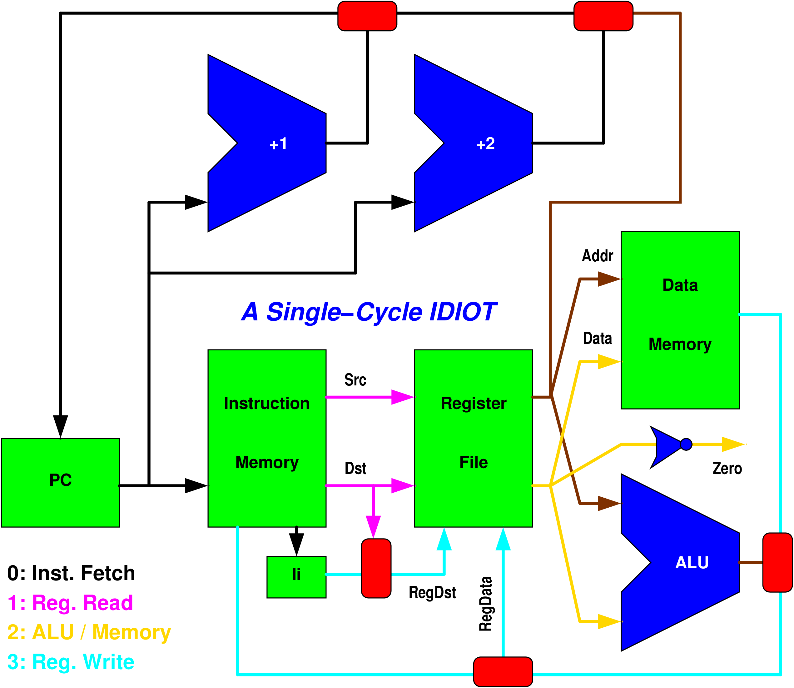
I could ask you to design your own single-cycle implementation from scratch, but I'll save us all some time and give you an overview diagram for such a thing right here:
You should recognize this from my little walk-through in class on March 25, but I have re-drawn it much neater, as I said I would. It's also color coded. Registers and other memory units are green, things that compute values are blue, and multiplexors are red. I'm not going to go through the wholen lecture again here, but the key ideas were:
Well, that wasn't so bad now, was it? Well, of course not... because that's not what you have to do. You have to make a pipelined design.
One of the first steps in making a pipelined implementation is figuring-out how many stages there should be and what belongs in each. You may have noticed that the function units are not all that is colored in the above diagram -- well, the other colors are a hint about how to pipeline.
It is fairly obvious that the memories will take a little while to access, and we all know ALUs are notoriously slow. Thus, we'd expect a stage for each of those things along any circuit path. Roughly speaking, that means the black wires are active during the first stage as the instruction is fetched, the magenta wires are active as the register file reads the two register values (which requires a register file capable of two reads in one clock cycle), the gold/brown wires are active during the third cycle when the main ALU for data memory is used, and the cyan wires are active while writing into the destination register. This fairly obviously leads to a 4-stage pipeline: Instruction Fetch to Register Read to ALU / Memory access to Register Write.
See? Now that wasn't so bad, was it? Of course not... but your task is a little harder. The ALU instructions and load and store are all easy, and sys is still just halt, but that leaves three instructions with issues. How can you deal with them?
Let's be completely clear about what I expect: your submission
should be a four-or-more-stage pipelined Verilog implementation
of IDIOT's non-floating-point instruction set. I expect you to
implement both sz and jz in a way where there
is some circumstance (e.g., non-zero) in which the instruction
does not cause a pipeline bubble. I also expect you to correctly
handle li operations, but have no problem at all with
each
Assignment 2 was scary, but that was because you had never done
something like this before -- now you have. For this project,
you are allowed to reuse any pieces from the Assignment 2
solutions that you, or any of your Assignment 3 teammates.
helped create. You also may use any materials I give you here.
Perhaps most importantly, you also are free to not use
any of those things; in other words, you can combine any of
those materials and make changes as your Assignment 3 team sees
fit. For example, if you don't like the way instruction fields
are encoded, feel free to re-write the AIK assembler (but make
sure your Implementor's Notes documents how instructions are
encoded and why).
In general, you are not allowed to use anything from
another Assignment 3 team nor from an Assignment 2 team that
none of your Assignment 3 team members were on. You
can use things done by any of your Assignment 3 team members,
including things their teams did on Assignment 2, and things
provided as part of this assignment. So, let's start the
giving....
Here's my sample Assignment 2 solution for an AIK specification:
It will encode instructions the way I discussed in class, which
you are free to use or not use. There are several "clever"
opcode grouping decisions embodied in it. All the ALU
instructions have at least one of the top two opcode bits as 0
-- i.e., all the non-ALU instructions match the opcode pattern
4'b11xx. Within the ALU instructions, you'll see
4'b00xx is used for arithmetic, 4'b01xx for
logical, and 4'b10xx for single-operand
transformations. Similarly, load and store encode as
4'b110x. The control flow operations are all
4'b1110 and li (which is almost a control flow
operation because it is two words long) is encoded by
4'b1111. The selection of how to encode the argument
register numbers is obvious in the above AIK specification...
with the key property being consistency of the hardware's use of
the values in each of the fields.
Although I strongly encourage you to make separate modules at
least for the main memory and ALU, here's my scary-simple
multi-cycle Verilog design for Assignment 2:
As discussed in class, the above Verilog code is very likely to
result in a bigger circuit than if we carefully factored things
into modules and created single instances of those modules. For
example, a Verilog compiler processing the above might fail to
map mainmem into a dedicated memory block within an
FPGA, instead constructing a memory using thousands of logic
cells. Using an instance of a memory module designed to comply
with the FPGA-maker's guidelines (e.g., this dual-port RAM with a Single Clock from ALTERA) ensures
that the vendor's Verilog toolchain will correctly infer use of
the intended hardware modules inside the FPGA. Of course, in
this class we are not rendering designs into physical circuits,
so these issues of complexity (and timing analysis) are neither
obvious nor critical... but you should always be aware of the
potential hardware complexity you risk introducing by using a
specification style that doesn't explicitly factor-out the
desired modules.
So, does the above Verilog code work? Mostly... which means
"no." What's wrong? Well, the same thing that is wrong with the
abstract single-cycle diagram up above: a sz will not
correctly skip over a li instruction. In fact, it is a
pain to fix that in the above Verilog code... so consider this a
good example of where documenting a bug might actually make
more sense than trying to fix it. How could one fix it?
Basically, you'd have to actually fetch the skipped instruction
and look at the opcode field, skipping a second word if opcde
field was `OPli. I'll leave the actual Verilog code as
an exercise for the reader (that means you ;-) ).
Ok, so that was roughly an Assignment 2 solution... what about
the single-cycle design? Well, it doesn't have to be much
different. The biggest difference is chaining everything
together as one state, whereas the above took three states.
The main trick is to absorb `Start and `Start1.
That's easily done, except for the little detail that you need
to override the state choice if you're fetching the second word
of an li.
Again, the test coverage plan and testbench from Assignment 2
are probably very close to what you want. However, you do need
to seriously think about coverage again. Why? You are not
testing the same Verilog code, so there may be some paths that
didn't exist before -- and they might not be covered with a
testbench that covered your old version.
In general, you'd need to write a lot of Verilog code to
implement a testbench for a complex circuit. However, as I
reminded you in class, here you are building a processor -- so
it can actually execute much of its own testing. All we need to
do is execute a test program and have code examine the results.
This approach has the happy benefit of also being a viable way
to test that the actual hardware correctly implements the
design: you would just run the code on the actual hardware.
A testbench to execute whatever program until completion is:
This just enables trace generation, intializes everything with a
reset, and then keeps toggling the clk until
the processor says it has reached a halted state.
Next, you need some code to run on it. For example:
This code tests quite a lot (although not sz skipping a
li!), but we'd have to look at a lot of register
contents to see if everything is right. That's a tad awkward
because the registers are hidden away inside the processor.
However, they are not hidden from code being simulated on the
processor, so we could simply add code to check the register
values... but then how would I know it succeeded? The answer is
a very simple trick: look at where the PC was when it halted
(i.e., hopefully when it executed the sys instruction).
In the above sequence, it should stop with the PC pointing at
good -- if it stopped anywhere else, something did not
work right.
Ah, but that doesn't test the values, does it? Nope. Here's how
we test. For example, u3 should end-up being
0x5335, so we simply compare and execute a sys
instruction if the value is not as desired. Executing the
sys instruction will halt the machine, leaving the PC
pointing to the failed test case! The sequence would look like:
Of course, you can write IDIOT processor code that tests
anything -- not just values in registers.
The recommended due date is Wednesday, April 13. Final submissions will be accepted up to when
class begins on Monday, April 18 (extended from 11:59PM on
Sunday, April 17 as announced in class).
Each team will submit a project tarball (i.e., a file
with the name ending in .tar or .tgz) that
contains all things relevant to your work on the project.
Minimally, each project tarball includes the source code for the
project and a semi-formal "implementors
notes" document as a PDF named
notes.pdf.
(Fairly obviously, the Implementor's Notes should also
say who the implementors are -- list all team members as
authors.)
It also may include test
cases, sample output, a make file, etc., but should not include
any files that are built by your Makefile (e.g., no binary
executables). For this particular project, name the Verilog
source file pipe.v.
Submit your tarball below. The file can be
either an ordinary .tar file created using tar cvf
file.tar yourprojectfiles or a compressed
.tgz file file created using tar zcvf
file.tgz yourprojectfiles. Be careful
about using * as a shorthand in listing
yourprojectfiles on the command line, because
if the output tar file is listed in the expansion, the result
can be an infinite file (which is not ok).
Use the submission form below to submit your project
as a single submission for your team --
you do not submit as individuals.
The last submission before the final deadline is the
one that will be graded.
Stuff You Can Reuse
Instruction Encoding And AIK Specification
; AIK definition of IDIOT assembler, 20160321 by H. Dietz
add  $.d,$.s := 0b0000:4 .d:6 .s:6
and  $.d,$.s := 0b0100:4 .d:6 .s:6
any  $.d,$.s := 0b0111:4 .d:6 .s:6
dup  $.d,$.s := 0b1000:4 .d:6 .s:6
jz   $.d,$.s := 0b1110:4 .d:6 .s:6
ld   $.d,$.s := 0b1100:4 .d:6 .s:6
li   $.d,.v  := 0b1111:4 .d:6  0:6 .v:16
or   $.d,$.s := 0b0101:4 .d:6 .s:6
sz   $.d     := 0b1110:4 .d:6  1:6
shr  $.d,$.s := 0b1001:4 .d:6 .s:6
st   $.d,$.s := 0b1101:4 .d:6 .s:6
sys          := 0b1110:4  0:6  0:6
xor  $.d,$.s := 0b0110:4 .d:6 .s:6
addf $.d,$.s := 0b0010:4 .d:6 .s:6
f2i  $.d,$.s := 0b1010:4 .d:6 .s:6
i2f  $.d,$.s := 0b1011:4 .d:6 .s:6
invf $.d,$.s := 0b0001:4 .d:6 .s:6
mulf $.d,$.s := 0b0011:4 .d:6 .s:6
.const {zero	one	sign	all	sp	fp	ra	rv
	u0	u1	u2	u3	u4	u5	u6	u7
        u8  	u9	u10	u11	u12	u13	u14	u15
        u16  	u17	u18	u19	u20	u21	u22	u23
        u24 	u25	u26	u27	u28	u29	u30	u31
        u32 	u33	u34	u35	u36	u37	u38	u39
        u40 	u41	u42	u43	u44	u45	u46	u47
        u48 	u49	u50	u51	u52	u53	u54	u55 }
.segment .text 16 0x10000 0 .VMEM
.segment .data 16 0x10000 0x8000 .VMEM ; default data start at 0x8000
.const 0 .lowfirst ; was wrong endian for li
Verilog Implementations
// basic sizes of things
`define WORD	[15:0]
`define Opcode	[15:12]
`define Dest	[11:6]
`define Src	[5:0]
`define STATE	[4:0]
`define REGSIZE [63:0]
`define MEMSIZE [65535:0]

// opcode values, also state numbers
`define OPadd	4'b0000
`define OPinvf	4'b0001
`define OPaddf	4'b0010
`define OPmulf	4'b0011
`define OPand	4'b0100
`define OPor	4'b0101
`define OPxor	4'b0110
`define OPany	4'b0111
`define OPdup	4'b1000
`define OPshr	4'b1001
`define OPf2i	4'b1010
`define OPi2f	4'b1011
`define OPld	4'b1100
`define OPst	4'b1101
`define OPjzsz	4'b1110
`define OPli	4'b1111

// state numbers only
`define OPjz	`OPjzsz
`define OPsys	5'b10000
`define OPsz	5'b10001
`define Start	5'b11111
`define Start1	5'b11110

// source field values for sys and sz
`define SRCsys	6'b000000
`define SRCsz	6'b000001

module processor(halt, reset, clk);
output reg halt;
input reset, clk;

reg `WORD regfile `REGSIZE;
reg `WORD mainmem `MEMSIZE;
reg `WORD pc = 0;
reg `WORD ir;
reg `STATE s = `Start;
integer a;

always @(reset) begin
  halt = 0;
  pc = 0;
  s = `Start;
  $readmemh0(regfile);
  $readmemh1(mainmem);
end

always @(posedge clk) begin
  case (s)
    `Start: begin ir <= mainmem[pc]; s <= `Start1; end
    `Start1: begin
             pc <= pc + 1;            // bump pc
	     case (ir `Opcode)
	     `OPjzsz:
                case (ir `Src)	      // use Src as extended opcode
                `SRCsys: s <= `OPsys; // sys call
                `SRCsz: s <= `OPsz;   // sz
                default: s <= `OPjz;  // jz
	     endcase
             default: s <= ir `Opcode; // most instructions, state # is opcode
	     endcase
	    end

    `OPadd: begin regfile[ir `Dest] <= regfile[ir `Dest] + regfile[ir `Src]; s <= `Start; end
    `OPand: begin regfile[ir `Dest] <= regfile[ir `Dest] & regfile[ir `Src]; s <= `Start; end
    `OPany: begin regfile[ir `Dest] <= |regfile[ir `Src]; s <= `Start; end
    `OPdup: begin regfile[ir `Dest] <= regfile[ir `Src]; s <= `Start; end
    `OPjz: begin if (regfile[ir `Dest] == 0) pc <= regfile[ir `Src]; s <= `Start; end
    `OPld: begin regfile[ir `Dest] <= mainmem[regfile[ir `Src]]; s <= `Start; end
    `OPli: begin regfile[ir `Dest] <= mainmem[pc]; pc <= pc + 1; s <= `Start; end
    `OPor: begin regfile[ir `Dest] <= regfile[ir `Dest] | regfile[ir `Src]; s <= `Start; end
    `OPsz: begin if (regfile[ir `Dest] == 0) pc <= pc + 1; s <= `Start; end
    `OPshr: begin regfile[ir `Dest] <= regfile[ir `Src] >> 1; s <= `Start; end
    `OPst: begin mainmem[regfile[ir `Src]] <= regfile[ir `Dest]; s <= `Start; end
    `OPxor: begin regfile[ir `Dest] <= regfile[ir `Dest] ^ regfile[ir `Src]; s <= `Start; end

    default: halt <= 1;
  endcase
end
endmodule
Testing
module testbench;
reg reset = 0;
reg clk = 0;
wire halted;
processor PE(halted, reset, clk);
initial begin
  $dumpfile;
  $dumpvars(0, PE);
  #10 reset = 1;
  #10 reset = 0;
  while (!halted) begin
    #10 clk = 1;
    #10 clk = 0;
  end
  $finish;
end
endmodule
  .data
test:
  .word 0x601
  .text
main:
  li   $u0,0x1003
  add  $u0,$one ; u0=0x1004
  li   $u1,0x4321
  li   $u2,0x1234
  and  $u1,$u2 ; u1=0x0220
  li   $u3,0x4321
  or   $u2,$u3 ; u2=0x5335
  li   $u4,0x1234
  xor  $u3,$u4 ; u3=0x5115
  any  $u4,$u4 ; u4=1
  any  $u5,$zero ; u5=0
  dup  $u6,$sign ; u6=0x8000
  li   $u7,0x8421
  shr  $u7,$u7 ; u7=0x4210
  li   $u8,test ; u8=0x8000
  li   $u9,0x0042 ; u9=0x0042
  st   $u9,$u8 ; test=42
  ld   $u10,$u8 ; u10=0x0042
  dup  $u11,$zero ; u11=0
  li   $u12,taken
  jz   $u11,$u12
  dup  $u11,$one ; should not happen
taken:
  dup  $u12,$one
  li   $u13,nottaken
  jz   $u12,$u13
  dup  $u12,$all ; u12=0xffff
nottaken:
  sz   $u13
  dup  $u13,$zero ; u13=0x0000
  dup  $u14,$zero ; u14=0x0000
  sz   $u14
  dup  $u14,$one
  dup  $u15,$zero ; u15=0x0000
  sys
good:
  dup  $u15,$all ; should not execute
  li   $u55,0x5335
  xor  $u55,$u3     ;compare for equality
  sz   $u55
  sys               ;if the buck stopped here, bad!
Due Dates
Submission Procedure
![]() Advanced Computer Architecture.
Advanced Computer Architecture.